Transparent conductive films are an important part of many optoelectronic devices, such as flat panel displays, organic solar cells, organic light emitting diodes (OLEDs), smart windows, and the like. Indium tin oxide (ITO) has become the main material of transparent conductive films due to its high electrical conductivity and light transmittance. However, ITO also has some disadvantages, such as the rising price of raw material indium, which is expensive to prepare, and in addition, once the ITO material is bent, its electrical conductivity is greatly reduced. Therefore, it is extremely important to develop new materials that can replace ITO. Currently, transparent conductive materials that are expected to replace ITO are doped with ZnO, carbon nanotubes, graphene, metal lanthanum and metal nanowires. Among them, carbon nanotubes, graphene, and silver and copper have attracted much attention in terms of flexibility, stability, and electrical conductivity. Among these alternative materials, silver and copper nanowires in metal nanowires can meet the material requirements of future optoelectronic devices due to their good electrical, mechanical and chemical properties. Under the current circumstances, scientists have prepared a copper nanowire growth process that has the potential to reduce the manufacturing cost of displays such as mobile phones and e-readers, and also help scientists build foldable electronic products and improve the performance of solar cells. The light transmittance and film resistance of the two are very close to each other. The copper content is very rich compared with silver nanowires and ITO, and the price is 100 times cheaper. The low price and abundant storage of copper nanowires make the research of copper nanowires equally important, so it is regarded as one of the most promising flexible transparent electrode materials. The preparation of transparent conductive films using copper nanowires is an ideal development path. In addition, due to the large aspect ratio effect of copper nanowires, it also has outstanding advantages in the application of conductive adhesives and thermal conductive adhesives.
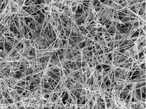
Here is the specification of copper nanowires from our company:
Diameter:50-200nm, length:1-10um, purity is 99%
Copper nanowire application types:
(1) Application in catalysis
Copper nanowires have excellent catalytic activity and reaction selectivity, which can improve the reaction efficiency. Therefore, their catalytic activity is much more selective than conventional catalysts and is used as a catalyst for various reactions.
(2) Application in the field of optics
Copper nanowires have excellent photoelectric effect, and due to the ultra-fast nonlinear optical response near the surface plasmon absorption peak, composites prepared by doping copper nanowires in semiconductors or insulators can achieve higher photoexcitation. Rate and extremely strong third-order nonlinear polarizability coefficients. These optical properties make copper nanowires widely used in the field of optics.
(3) Application in the field of electrodes
ITO is currently the most widely used transparent electrode material for flat panel display, touch screen, PDP display and related technologies. However, the material is relatively brittle and has a high preparation temperature, which is expensive, mainly because it requires indium which is scarce in surface growth. In addition to excellent electrical conductivity, copper nanowires have excellent light transmission and low cost. And copper nanowires are entirely possible to achieve large-area material preparation through the spraying process, and are regarded as one of the most potential flexible transparent electrode materials.
(4) Applications in other fields
Due to the large aspect ratio effect of copper nanowires, the ultra-high electrical and thermal conductivity also has outstanding advantages in the application of conductive paste, conductive adhesive, thermal conductive adhesive and the like.


 online service
 13929258449
 admin@satnano.com
 + 8613929258449


