
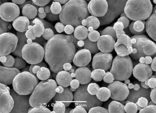
Scanning electron microscope (SEM) is a key tool for modern scientific exploration of the microscopic world. It plays an irreplaceable role in scientific research and industrial applications by enabling us to gain insights into the microscopic structure of matter through high-resolution electronic imaging technology. SEM scans the surface of the sample with a high-energy electron beam to collect signals generated by the interaction between electrons and the sample, including secondary electrons, backscattered electrons, and X-rays, in order to obtain detailed morphology, composition, and structural information of the sample surface. This technology provides higher resolution than traditional optical microscopes, allowing observation of nanoscale microstructures such as nanoparticles, viruses, and organelles.
Components and imaging process of SEM
SEM consists of main components such as electron gun, electromagnetic lens, scanning coil, sample chamber, and detector. The electron gun generates an electron beam, which is focused into small probes by an electromagnetic lens. The scanning coil controls the scanning path of the electron beam on the surface of the sample. The detector receives and converts the signal generated by the interaction between electrons and the sample, and finally generates an image on the display. By adjusting the parameters of the electron beam and the detector settings, different information about the sample can be obtained. Jinjian Laboratory has rich experience in this area and can provide professional guidance for customers in sample preparation and imaging processes, ensuring the acquisition of high-quality images and accurate analysis results.
Key operating parameters of SEM
1. Acceleration voltage: It affects the energy and penetration ability of the electron beam and needs to be selected based on the characteristics of the sample. 2. Working distance: It affects the focusing and resolution of the electron beam and needs to be adjusted according to experimental requirements. 3. Sample preparation: It is an important step in SEM analysis, and different samples require different preparation methods to ensure image quality and accuracy of analysis results. Jinjian Laboratory provides professional sample preparation services to ensure that the processing of different types of samples meets experimental requirements, thereby improving image quality and accuracy of analysis results.
The Importance of Sample Preparation
Sample preparation is crucial for SEM analysis. Conductive samples can be directly observed, while non-conductive samples may require gold or carbon spraying treatment to improve conductivity. Biological samples typically require steps such as fixation, dehydration, drying, and may require gold spraying to enhance their conductivity and stability.
The Wide Application of SEM
1. Materials Science: Used to characterize the microstructure, crystal structure, and chemical composition of materials, such as fracture analysis of metal materials, microstructure of alloys, and grain structure of ceramic materials. 2. Microelectronics and Semiconductors: Detecting manufacturing defects in integrated circuits, analyzing device failure mechanisms, and characterizing the structure of nanodevices. 3. Biomedicine: Observing the surface morphology, tissue structure, and surface properties of biological materials. 4. Environmental science: Analyze the morphology, composition, and sources of environmental samples, such as atmospheric particulate matter and water sediment. 5. Archaeology and cultural relic protection: Analyze the structure, composition, and microscopic morphology of ancient bones and teeth of cultural relics. SEM is not only a super eye for exploring the microscopic world, but also an important tool in scientific research. It enables us to delve into the internal structure of matter, revealing hidden details, thereby driving scientific development and technological innovation in multiple fields. Jinjian Laboratory is committed to providing customers with the most professional SEM analysis services, promoting scientific development and technological innovation, and providing strong support for research in various fields.


 online service
 13929258449
 admin@satnano.com
 + 8613929258449


