


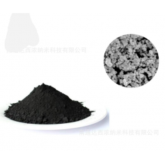
CAS 7440-05-3 Pd nanopowder Ultrafine Palladium as catalyst
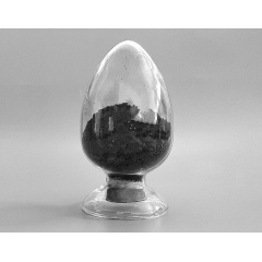
Size:20-30nm Purity:99.95% CAS No:7440-05-3 ENINEC No.:231-115-6 Appearance:black Powder Shape:spherical

Size:20-30nm Purity:99.95% CAS No:7440-05-3 ENINEC No.:231-115-6 Appearance:black Powder Shape:spherical
We can supply different size products of niobium silicide powder according to client's requirements. Size:1-3um; Purity:99.5%;Shape:granular CAS No:12034-80-9;ENINEC No.:234-812-3
Ni2Si particle,99.5% purity,granular shape,is used for Microelectronic integrated circuit, nickel silicide film,etc. Size:1-10um; CAS No:12059-14-2;ENINEC No.:235-033-1
Buy conductive copper oxide powder for nano copper oxide film, Size 20nm, 40nm, 100nm, 1-3um, 10um. Purity:99.9%. Please click it to check the specification
Brand:
SAT NANOItem NO.:
OP2908-50NPayment:
TT, Paypal, WUProduct Origin:
ChinaColor:
Black PowderShipping Port:
Shenzhen, ShanghaiLead Time:
1-5daysMin Order:
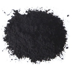
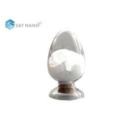
1kgSpecification of copper oxide nanopowder:
Size: 50nm particle
CAS No:1317-38-0
ENINEC No.:215-269-1
Appearance:black Powder
Shape:spherical
Note: We can supply different size products of copper oxide nanoparticle according to client's requirements.
SAT NANO also supply other size particle like 20nm, 40nm, 100nm, 1-3um, 10um.
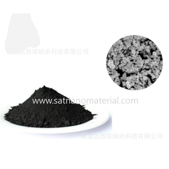
The 50nm spherical nano-copper oxide is produced by a low-temperature active process. The 50nm spherical nano-copper oxide has the advantages of high activity, soft agglomeration, low heavy metal impurities, and good dispersion performance. At the same time, because of its own characteristics, the 50nm spherical nano-copper oxide is widely used in catalysis, Sterilization and other fields.
Application of Nano Copper Oxide Film
Nano copper oxide film has good transparent conductivity, piezoelectricity, photoelectricity, gas sensitivity, pressure sensitivity, and is easy to integrate with a variety of semiconductor materials. Due to these excellent properties, it has a wide range of uses and many potential applications, such as optoelectronic devices, surface acoustic wave devices, planar optical waveguides, transparent electrodes, transparent conductive films, piezoelectric devices, gas sensors and GaN buffer layers Wait.
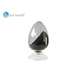
Size:50nm, 80nm, 1-2um, 5um Purity:99.9% CAS No:1317-38-0 ENINEC No.:215-269-1 Appearance:black Powder Shape:Spherical
Size:50nm, 80nm, 1-2um, 5um Purity:99.9% CAS No:1317-38-0 ENINEC No.:215-269-1 Appearance:black Powder Shape:Spherical
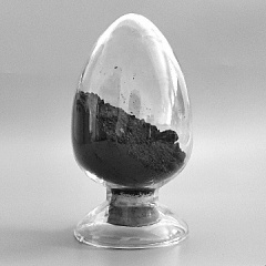
Size:50nm, 80nm, 1-2um, 5um Purity:99.9% CAS No:1317-38-0 ENINEC No.:215-269-1 Appearance:black Powder Shape:Spherical
Size:50nm, 80nm, 1-2um, 5um Purity:99.9% CAS No:1317-38-0 ENINEC No.:215-269-1 Appearance:black Powder Shape:Spherical
20nm black copper oxide nanopowder as additive, Purity:99.9%. It has a better anti-mold effect in the application of polyester materials. Please click it to check the specification
50nm copper oxide nanopowder, little addition, strong antibacterial ability, Purity:99.9%. Please click it to check the specification
30nm Rod-shaped copper oxide to treat sulfur-based malodorous gas, strong antibacterial ability, Purity:99.9%. Please click it to check the specification
Buy 50nm spherical black copper oxide nanopowder factory price for sale, strong antibacterial ability, Purity:99.9%. Please click it to check the specification
Buy copper oxide CuO used for Catalytic oxidation of volatile organic compounds, strong antibacterial ability, Purity:99.9%. Please click it to check the specification
Buy atomized copper oxide powder with High specific surface area, Size 20nm, 40nm, 100nm, 1-3um, 10um. Purity:99.9%. Please click it to check the specification
Buy conductive copper oxide powder used in battery, Size 20nm, 40nm, 100nm, 1-3um, 10um. Purity:99.9%. Please click it to check the specification
Buy Zinc Oxide Nano Powder Nano ZnO Nanoparticles 20nm, Purity:99.8%, high quality, low price, and fast delivery, please click it to check the specification.


 online service
 13929258449
 admin@satnano.com
 + 8613929258449