


CAS 7440-05-3 Pd nanopowder Ultrafine Palladium as catalyst
Size:20-30nm Purity:99.95% CAS No:7440-05-3 ENINEC No.:231-115-6 Appearance:black Powder Shape:spherical

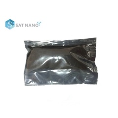
Size:20-30nm Purity:99.95% CAS No:7440-05-3 ENINEC No.:231-115-6 Appearance:black Powder Shape:spherical
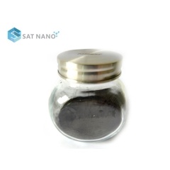
We can supply different size products of niobium silicide powder according to client's requirements. Size:1-3um; Purity:99.5%;Shape:granular CAS No:12034-80-9;ENINEC No.:234-812-3
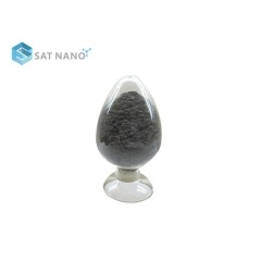
Ni2Si particle,99.5% purity,granular shape,is used for Microelectronic integrated circuit, nickel silicide film,etc. Size:1-10um; CAS No:12059-14-2;ENINEC No.:235-033-1
Perovskite quantum dots have the advantages of high color purity, high radiation recombination efficiency, and solution processability, making them naturally suitable for high-end displays and microdisplay devices. However, there is always a bottleneck in truly transforming "superlattice orderliness" into "device performance advantages". How to simultaneously achieve long-range in-plane ordering, ultra-thin vertical confinement, and pixel level precise patterning has always been a problem that needs to be solved.
Recently, the journal Nature reported that researchers proposed a ligand fluoride co stabilization strategy to synergistically regulate the surface of CsPbBr3 quantum dots using the tertiary ammonium ligand BHOA and tetrabutylammonium fluoride (TBAF). CsPbBr3 perovskite quantum dots with high geometric symmetry, narrow size distribution, and strong surface binding ability were synthesized in a rhombic dodecahedron morphology. Pixelated perovskite quantum dot superlattice thin film arrays were successfully prepared using capillary liquid bridge confinement assembly technology.
Benefiting from stronger surface binding, the photoluminescence quantum yield of BHOA+F quantum dot solution reached 94.6%, and the complete luminescence intensity could still be maintained after 72 hours of air aging at 60 ℃; The T90 of the corresponding thin film under air and ultraviolet irradiation exceeded 700 hours, much higher than the 4 hours of the OLA system. Subsequently, the authors used capillary liquid bridge restricted assembly to induce localized crystallization of quantum dots in micro column templates, obtaining a pixelated superlattice thin film with a thickness of about 25 nm and a thickness of about two layers of quantum dot monolayers.
Compared with the spin coating control, the superlattice film exhibits better structural and optoelectronic properties: the transient absorption bleaching peak linewidth decreases from 93.6meV to 70.1meV, the bleaching peak position drift Δ E decreases from 17.4meV to 8.9meV, the steady-state emission half width narrows from 19.4nm to 17.1nm, the absolute PLQY of the film increases from 68.8% to 82.3%, the conductivity increases from 2.01 × 10⁻⁴Sm-1 to 4.52 × 10⁻⁴Sm-1, and a band transport characteristic of d μ/dT<0 appears below 188K.
To verify the potential of practical display applications, the research team directly integrated superlattice arrays with commercial low-temperature polycrystalline silicon thin film transistor backplates, and fabricated an active matrix display screen with a resolution of 300 PPI and a size of 1.85 inches. The turn-on voltage of pixelated superlattice LED decreased from 2.4V to 2.2V, the peak external quantum efficiency (EQE) reached 30.9%, the maximum brightness reached 117144cd m-2, and the highest resolution reached 5080PPI; Among the 40 device statistics, the average EQE reached 27.4%, significantly higher than the 21.7% of the spin coating control. More importantly, the device extrapolated T50 to 12411 hours at 100cd m-2, which is more than 1000 times longer than the reported pixelated PeQD LED lifespan, and further demonstrated an active matrix display of 1.85 inches, 352 × 430 pixels, and 300PPI.
The pixelated superlattice light-emitting diode constructed by this work not only broke the records of similar devices in terms of efficiency, brightness, and lifespan, but more importantly, the process is fully compatible with photolithography patterning and commercial thin-film transistor backplates, providing a feasible material system and manufacturing solution for the next generation of high-resolution and high stability perovskite display technology.


 online service
 13929258449
 admin@satnano.com
 + 8613929258449